

How Semiconductor Doping Controls Conductivity Explainer
A pure semiconductor conducts better than an insulator but worse than a metal because only a limited number of electrons can move into available energy states. Doping deliberately replaces a small fraction of crystal atoms with impurities that change this carrier population. The useful explanation follows energy and charge while respecting the material properties at each boundary.
In silicon, a donor atom with an extra valence electron can release that electron relatively easily, producing n-type material. An acceptor with one fewer valence electron leaves a mobile absence called a hole, producing p-type material. Geometry and composition set the available pathways, so small design changes can alter the response.
Electrons and holes respond in opposite directions to an electric field, yet both carry current through the crystal. Dopant concentration shifts the Fermi level and changes conductivity, while temperature determines how many dopants are ionized and how often carriers scatter. The process continues only while a driving difference overcomes losses, resistance, or competing motion.
Joining p-type and n-type regions forms a depletion zone where carriers recombine and fixed dopant ions create an internal electric field. External voltage can narrow or widen that barrier, enabling rectification, switching, sensing, light emission, or photovoltaic conversion. Real devices add interfaces and imperfections that idealized diagrams usually leave out.
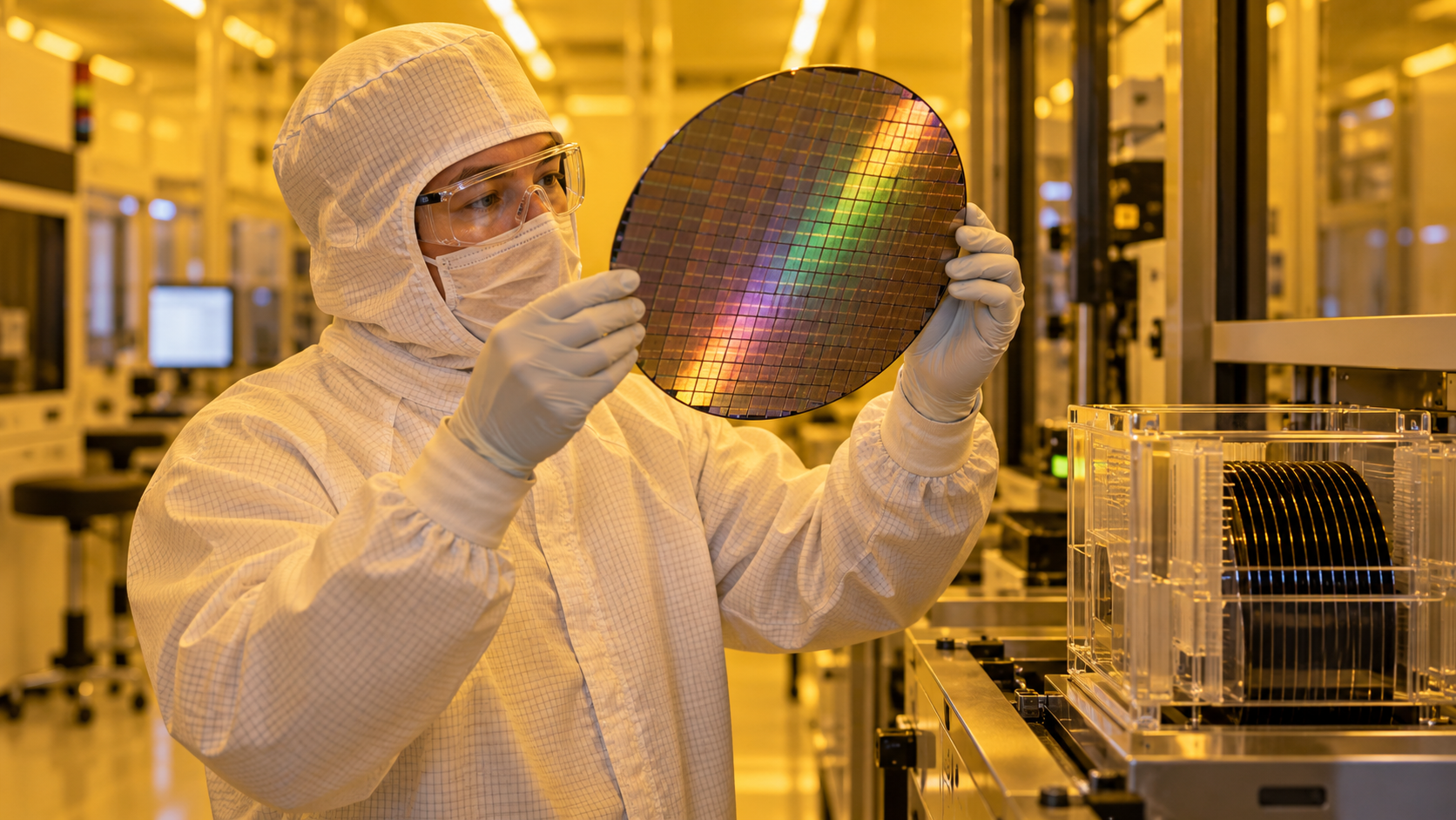
Fabrication uses diffusion, ion implantation, and carefully controlled heating to place dopants at selected depths. Hall measurements and other electrical tests reveal carrier type, density, mobility, and uniformity, while microscopy checks damage and interface structure. Scientists test the model by changing one condition and measuring the predicted optical, thermal, or electrical signal.
More dopant does not always mean a proportionate improvement. High concentrations can increase scattering, introduce defects, or alter junction behavior. Modern electronics depend on controlling profiles across nanometer-scale regions, not merely making an entire wafer more conductive. The core physics is dependable, but efficiency and scale depend on engineering details and operating conditions.
Pure semiconductors have relatively few mobile charge carriers.
Donor dopants add easily released electrons and create n-type material.
Acceptor dopants create mobile holes and produce p-type material.
Carrier density and mobility together determine conductivity.
P-n junction fields make one-way transport and switching possible.
Excess doping can raise scattering and damage device performance.
Explore more "Explainers"
Discover additional explainers across politics, science, business, technology, and other fields. Each explainer breaks down a complex idea into clear, everyday language—helping you better understand how major concepts, systems, and debates shape the world around us.